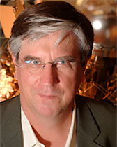
Michael J. Bedzyk
· Professor of Materials Science and Engineering and (by courtesy) Physics and AstronomyVerifiedNorthwestern University · Materials Science and Engineering
Active 1975–2026
About
Professor Michael J. Bedzyk is the Principal Investigator of the Bedzyk Research Group and holds the position of Professor of Materials Science & Engineering by courtesy at Northwestern University. He also serves as the Co-Director of the Northwestern Synchrotron Research Center. His office is located in Cook Hall Room 1139 at Northwestern University. The information provided highlights his leadership role within the research group and his involvement in advanced materials science research, particularly utilizing synchrotron radiation facilities. The page lists numerous current and former group members, indicating a long-standing and active research program under his guidance. However, the page text does not provide specific details about his research focus, background, or key scientific contributions beyond his academic and administrative titles and affiliations.
Research topics
- Materials science
- Chemistry
- Nanotechnology
- Electrical engineering
- Optoelectronics
- Metallurgy
- Physical chemistry
- Crystallography
- Chemical engineering
- Chemical physics
- Optics
- Composite material
- Organic chemistry
Selected publications
ArXiv.org · 2026-02-07
articleOpen accessNiobium metal occupies nearly 100\% of the volume of a typical 2D transmon device. While the aluminum Josephson junction is of utmost importance, maintaining quantum coherence across the entire device means that pair-breaking in Nb leads, capacitive pads, and readout resonators can be a major source of decoherence. The established contributors are surface oxides and hydroxides, as well as absorbed hydrogen and oxygen. Metal encapsulation of freshly grown surfaces with non-oxidizing metals, preferably without breaking the vacuum, is a successful strategy to mitigate these issues. While the positive effects of encapsulation are undeniable, it is important to understand its impact on the macroscopic behavior of niobium films. We present a comprehensive study of the bulk superconducting properties of Nb thin films encapsulated with gold and palladium/gold, and compare them to those of bare Nb films. Magneto-optical imaging, magnetization, resistivity, and London and Campbell penetration depth measurements reveal significant differences in encapsulated samples. Both sputtered, and epitaxial Au-capped films exhibit the highest residual resistivity ratio and superconducting transition temperature, as well as the lowest upper critical field, London penetration depth, and critical current. These results are in good agreement with the microscopic theory of anisotropic normal and superconducting states of Nb. We conclude that pair-breaking in the bulk of niobium films, driven by disorder throughout the film rather than just at the surface, is a significant source of quantum decoherence in transmons. We also conclude that gold capping not only passivates the surface but also affects the properties of the entire film, significantly reducing the scattering rate due to defects likely induced by surface diffusion if the film is not protected immediately after fabrication.
Surface Reordering During Layer‐by‐Layer Growth on SrTiO <sub>3</sub>
Advanced Materials · 2026-03-06
articleOpen accessABSTRACT With the development of layer‐by‐layer growth techniques such as molecular beam epitaxy (MBE), it is now possible to construct materials with atomic‐level precision, with the layer sequence primarily determined by the growth recipe. However, materials can still restructure in the high‐temperature growth environment with surface thermodynamics strongly influencing growth behavior. Here, we demonstrate that growth on (001), the principal platform for oxide electronics, does not occur in a layer‐by‐layer fashion but follows a more complex process in which a plane continually diffuses toward the growth surface. Employing in situ synchrotron X‐ray scattering combined with ab initio thermodynamic calculations, we discover the existence of a stable double‐layer structure on the pristine substrate and the occurrence of dynamic layer rearrangement during homoepitaxial growth by oxide MBE. Our findings suggest that the current methods used to precisely control surfaces are limited, as well as our ability to dictate the composition of ultrathin films, resulting in important ramifications regarding the surface reactivity of perovskite materials grown on .
Open MIND · 2026-02-07
preprintNiobium metal occupies nearly 100\% of the volume of a typical 2D transmon device. While the aluminum Josephson junction is of utmost importance, maintaining quantum coherence across the entire device means that pair-breaking in Nb leads, capacitive pads, and readout resonators can be a major source of decoherence. The established contributors are surface oxides and hydroxides, as well as absorbed hydrogen and oxygen. Metal encapsulation of freshly grown surfaces with non-oxidizing metals, preferably without breaking the vacuum, is a successful strategy to mitigate these issues. While the positive effects of encapsulation are undeniable, it is important to understand its impact on the macroscopic behavior of niobium films. We present a comprehensive study of the bulk superconducting properties of Nb thin films encapsulated with gold and palladium/gold, and compare them to those of bare Nb films. Magneto-optical imaging, magnetization, resistivity, and London and Campbell penetration depth measurements reveal significant differences in encapsulated samples. Both sputtered, and epitaxial Au-capped films exhibit the highest residual resistivity ratio and superconducting transition temperature, as well as the lowest upper critical field, London penetration depth, and critical current. These results are in good agreement with the microscopic theory of anisotropic normal and superconducting states of Nb. We conclude that pair-breaking in the bulk of niobium films, driven by disorder throughout the film rather than just at the surface, is a significant source of quantum decoherence in transmons. We also conclude that gold capping not only passivates the surface but also affects the properties of the entire film, significantly reducing the scattering rate due to defects likely induced by surface diffusion if the film is not protected immediately after fabrication.
Oxide-nitride heteroepitaxy for low-loss dielectrics in superconducting quantum circuits
arXiv (Cornell University) · 2026-03-30
articleOpen accessSenior authorSuperconducting qubits show great promise for the realization of fault-tolerant quantum computing, but lossy, amorphous dielectrics limit current technology. Identifying highly crystalline and stoichiometric dielectrics with intrinsically low microwave loss is therefore a central materials challenge, yet experimentally validated platforms remain scarce. In this work, we integrate a crystalline dielectric into a heteroepitaxial TiN/$γ$-Al$_2$O$_3$/TiN trilayer grown via pulsed laser deposition. Correlative high-resolution imaging, diffraction, and spectroscopy measurements confirm the single-crystal quality and chemical integrity of all layers, with minimal defects and limited anion interdiffusion across the oxide-nitride interfaces. Using microwave lumped-element resonators with parallel-plate capacitors, we report the first direct measurement of the dielectric loss of epitaxial $γ$-Al$_2$O$_3$, for which we find a low intrinsic two-level system loss, $δ_{\text{TLS}}^0 = (2.8 \pm 0.1) \times 10^{-5}$. These results establish heteroepitaxial oxides on transition metal nitrides as an attractive materials platform for superconducting quantum circuits, particularly for integration into compact device architectures such as merged-element transmons and microwave kinetic inductance detectors.
ACS Nano · 2026-03-04
articleNiobium thin films are central to superconducting qubits, but their complex native oxides contribute significantly to microwave losses. A promising mitigation strategy is to suppress oxide formation using engineered thin-film encapsulation layers. Recent experiments have shown that ∼10 nm metallic overlayers on Nb capacitor films can improve the energy relaxation time T1 of transmon qubits. Here, we present a comparative study of Au-capped Nb films fabricated in situ by molecular beam epitaxy and ex situ by sequential deposition benchmarked against bare Nb films. Using complementary structural, chemical, and spectroscopic techniques, we correlate the interface quality with superconducting electronic properties of the Au surface. Low-temperature scanning tunneling spectroscopy (STS) provides spatially resolved quasiparticle density-of-states maps. While both Au-capped Nb samples exhibit large areas with uniform, fully gapped density of states, clear differences emerge between the two interfaces. Compared to in situ Nb–Au, ex situ Nb–Au exhibits a reduced induced superconducting gap, broadened coherence peak, and localized in-gap states, consistent with a residual NbxOy layer at the interface. Supported by complementary structural and chemical analyses, these findings demonstrate that STS directly links nanoscale superconducting properties to interface preparation, highlighting the importance of controlled in situ encapsulation for minimizing dissipation and improving quantum coherence.
Oxide-nitride heteroepitaxy for low-loss dielectrics in superconducting quantum circuits
arXiv (Cornell University) · 2026-03-30
preprintOpen accessSenior authorSuperconducting qubits show great promise for the realization of fault-tolerant quantum computing, but lossy, amorphous dielectrics limit current technology. Identifying highly crystalline and stoichiometric dielectrics with intrinsically low microwave loss is therefore a central materials challenge, yet experimentally validated platforms remain scarce. In this work, we integrate a crystalline dielectric into a heteroepitaxial TiN/$γ$-Al$_2$O$_3$/TiN trilayer grown via pulsed laser deposition. Correlative high-resolution imaging, diffraction, and spectroscopy measurements confirm the single-crystal quality and chemical integrity of all layers, with minimal defects and limited anion interdiffusion across the oxide-nitride interfaces. Using microwave lumped-element resonators with parallel-plate capacitors, we report the first direct measurement of the dielectric loss of epitaxial $γ$-Al$_2$O$_3$, for which we find a low intrinsic two-level system loss, $δ_{\text{TLS}}^0 = (2.8 \pm 0.1) \times 10^{-5}$. These results establish heteroepitaxial oxides on transition metal nitrides as an attractive materials platform for superconducting quantum circuits, particularly for integration into compact device architectures such as merged-element transmons and microwave kinetic inductance detectors.
Desy Publications Database (Deutsches Elektronen-Synchrotron DESY) · 2025-01-01
articleOpen accessSenior authorHow do chemical and structural modifications to the supporting crystal surface affect the subsequent van der Waals (vdW) or quasi(Q)-vdW epitaxial growth of 2D nanocrystals? Developing an atomic-scale picture of such an interfacial system is crucial for understanding its impact on the physical and chemical properties of the supported 2D materials. The elucidation of the interfacial structure and chemistry needed to promote the Q-vdW epitaxial growth of 2D tungsten disulfide (WS$_2$) nanocrystals contributes to the growth mechanism understanding, thus pushing forward the integration of such atomically thin semiconductors toward real field-effect transistor applications. In addition to an atomic-force microscopy top view, we showcase a combination of X-ray techniques for a top-to-bottom investigation of the complexities of the buried interface structures. This approach uses X-ray photoelectron spectroscopy, X-ray standing wave excited X-ray fluorescence, and crystal truncation rod scattering to produce a highly resolved chemical-state-specific 3D atomic map for the extended interface structure of WS$_2$/α-Al$_2$O$_3$(001). Employing these detailed analysis methods, along with density functional theory to further refine the picoscale structure, we demonstrate how two different types of interface engineering during the pregrowth stage lead to significant differences in the chemical and structural modifications to the terminal surface of c-face sapphire, which in turn leads to substantial differences in the submonolayer growth of supported WS$_2$ 2D nanocrystals in terms of lateral domain sizes, epitaxial registry, vdW gaps, and stability.
Silver Copper Oxide: A p-Type Transparent Conductive Oxide?
ACS Applied Energy Materials · 2025-10-29 · 1 citations
articleIn this study, we report the room-temperature synthesis, detailed characterization, and first-principles modeling of monoclinic AgCuO2, a p-type transparent conducting oxide (TCO) candidate. AgCuO2 was synthesized via an oxidative coprecipitation method using Ag(I) and Cu(II) precursors in the presence of potassium persulfate as an oxidizing agent. Structural and morphological analyses, including powder X-ray diffraction, Rietveld refinement, high-resolution transmission electron microscopy, and atomic force microscopy, confirm the formation of a highly crystalline crednerite-type phase with minimal CuO impurity. Optical spectroscopy, combined with Kelvin probe, surface photovoltage spectroscopy, and UV photoemission measurements, reveals a direct optical bandgap of ∼2.5 eV and a Fermi level close to the valence band maximum, indicative of p-type semiconductor behavior. Importantly, the ambiguity of whether AgCuO2 is metallic or a semiconductor was resolved in the present study both by experiment and theory. Complementary electrochemical analyses demonstrated quasi-reversible redox activity and stability of the AgCuO2 surface, while conductivity measurements provided insight into the charge transport mechanism. Density functional theory (DFT + U) calculations corroborated the experimental findings, predicting a layered structure with Cu in a +3 oxidation state and revealing that Ag vacancy defects could enhance electrical conductivity without compromising optical transparency. This integrated experimental and computational approach establishes AgCuO2 as an electronically conductive, optically transparent, and electrochemically robust TCO candidate with potential for optoelectronic, photoelectrochemical, or solar photovoltaic applications.
ACS Applied Nano Materials · 2025-04-29
articleOpen accessSenior authorCorrespondingHow do chemical and structural modifications to the supporting crystal surface affect the subsequent van der Waals (vdW) or quasi(Q)-vdW epitaxial growth of 2D nanocrystals? Developing an atomic-scale picture of such an interfacial system is crucial for understanding its impact on the physical and chemical properties of the supported 2D materials. The elucidation of the interfacial structure and chemistry needed to promote the Q-vdW epitaxial growth of 2D tungsten disulfide (WS2) nanocrystals contributes to the growth mechanism understanding, thus pushing forward the integration of such atomically thin semiconductors toward real field-effect transistor applications. In addition to an atomic-force microscopy top view, we showcase a combination of X-ray techniques for a top-to-bottom investigation of the complexities of the buried interface structures. This approach uses X-ray photoelectron spectroscopy, X-ray standing wave excited X-ray fluorescence, and crystal truncation rod scattering to produce a highly resolved chemical-state-specific 3D atomic map for the extended interface structure of WS2/α-Al2O3(001). Employing these detailed analysis methods, along with density functional theory to further refine the picoscale structure, we demonstrate how two different types of interface engineering during the pregrowth stage lead to significant differences in the chemical and structural modifications to the terminal surface of c-face sapphire, which in turn leads to substantial differences in the submonolayer growth of supported WS2 2D nanocrystals in terms of lateral domain sizes, epitaxial registry, vdW gaps, and stability.
Coupling of Charge Regulation and Geometry in Soft Ionizable Molecular Assemblies
The Journal of Physical Chemistry B · 2025-04-08 · 1 citations
articleSenior authorCorrespondingThe size, shape, and charge of structures, such as proteins and amphiphile assemblies, respond in an interconnected manner to solution ionic conditions. We analyze assemblies of an amphiphile (C16K2), with two ionizable amino acids [lysine (K)] coupled to a 16-carbon alkyl tail, via small-angle X-ray scattering (SAXS), nonlinear Poisson–Boltzmann theory (nl-PB), and hybrid Monte Carlo-molecular dynamics (MC-MD) simulations. SAXS revealed structural transitions from spherical micelles to cylindrical micelles to bilayers with increasing pH. By combining SAXS-determined structural information and nl-PB, we derived the molecular degree of ionization as a function of pH. The back-calculated titration curves matched the experimental data over an extended pH range, without adjustable parameters. Similarly, the SAXS data on the evolution of spherical micelle structure with ionic strength were combined with nl-PB and MC-MD to derive the bare and effective charges. MC-MD, which considered finite ion sizes, showed that bare and effective charges saturate quickly with increasing salt concentration. Furthermore, the calculated effective charges closely matched results from Zeta-potential measurements. The presented approach has advantages over customary methods for charge regulation, such as the Henderson–Hasselbalch (HH) or Hill models, where molecular ionization/deionization in assemblies is described by effective pKs that are distinct from the pK for isolated molecules. However, these models lack a physical explanation for these pK shifts. By contrast, our approach of combining structural details with an electrostatic model and simulations provides a more intuitive understanding of structure-charge coupling and a framework for understanding charge regulation in many synthetic and biological systems.
Frequent coauthors
- 101 shared
Jeffrey A. Klug
- 94 shared
Tobin J. Marks
Northwestern University
- 91 shared
Mark C. Hersam
Northwestern University
- 86 shared
Paul Fenter
Argonne National Laboratory
- 84 shared
O. Auciello
- 83 shared
Darrell G. Schlom
Leibniz Institute for Crystal Growth
- 74 shared
Antonio Facchetti
Georgia Institute of Technology
- 68 shared
Ying‐Hao Chu
National Tsing Hua University
Labs
Atomic-Scale View of Interfacial Processes with X-rays
Education
Ph.D., Physics
State University of New York, Albany
B.S., Physics and Mathematics
State University of New York, Brockport
- Resume-aware match score
- Save to shortlist
- AI-drafted outreach
See your match with Michael J. Bedzyk
PhdFit ranks faculty by your research interests, methods, and publications — grounded in their actual work, not templates.
- Free to start
- No credit card
- 30-second signup